Semiconductor Metal Wiring Processes
Advancing Semiconductor Metal Wiring: Top Seiko’s Techniques
In semiconductor manufacturing, the metal wiring process is a crucial step.
This process creates tiny, conductive pathways across layers of a chip. These pathways act as the “nervous system” of electronics, letting transistors communicate and process information at high speeds. To achieve this, manufacturers rely on specialized materials like tungsten, titanium, alumina, and quartz.
Each one has a specific role in ensuring connectivity, insulation, and structural stability.
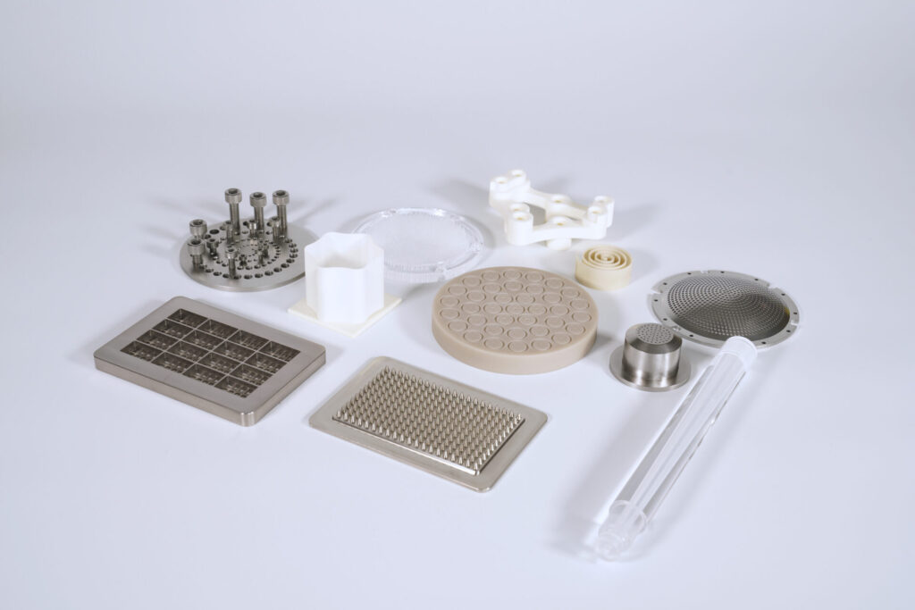
At Top Seiko, we specialize in precision machining of hard metals and ceramics.
Our high-quality components help manufacturers meet the exacting demands of semiconductor production.
Here’s a closer look at the metal wiring process and how Top Seiko’s custom solutions add value at each stage.
The Metal Wiring Process, Step by Step
Creating Contact Plugs:
Manufacturers use tungsten to form tiny plugs that connect different layers on the chip. This step requires extremely pure materials and precise components to keep resistance low and ensure reliable performance.Adding Barrier and Adhesion Layers:
Titanium and titanium nitride (TiN) provide essential layers that help the materials bond and prevent them from diffusing into each other. These layers ensure stability in the final product.Building Insulating Layers:
Alumina and quartz act as insulating layers between wiring. They keep signals clear and reduce power usage by preventing interference between the metal layers.Final Protection and Passivation:
These layers are topped with high-purity ceramics to protect the wiring from contaminants and keep the chip stable in tough conditions.
![]()
How Top Seiko Supports the Metal Wiring Process
Top Seiko provides custom-machined parts with exceptional precision, purity, and durability.
Our specialized components play a key role at each stage of the metal wiring process:
Precision in Tungsten and Titanium:
We deliver precision-machined tungsten and titanium components with exact dimensions and smooth surfaces. These high-quality parts fit seamlessly into semiconductor equipment, helping reduce contamination and maintain process purity.Advanced Alumina and Quartz Components:
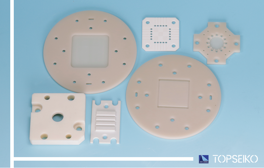
Alumina and quartz are ideal materials for insulation. We machine custom parts like wafer carriers and lithography plates with extreme accuracy. Our parts offer excellent electrical insulation, helping ensure that semiconductor manufacturers meet the strict standards required for reliable devices.Custom Parts for Prototyping and Scaling:
The semiconductor industry constantly innovates. Top Seiko supports this by providing rapid prototyping and custom part development, allowing manufacturers to test new processes without sacrificing precision or quality.
Why Choose Top Seiko?

Top Seiko’s experience with hard and brittle materials makes us a trusted partner in semiconductor manufacturing.
We create components that handle extreme temperatures and resist wear, corrosion, and contamination.
Our commitment to precision machining ensures that manufacturers can produce high-performance chips with confidence.
As technology advances, Top Seiko’s precision-machined materials offer the reliability and quality that semiconductor companies need to stay competitive. Our components help manufacturers produce cutting-edge microchips that power the latest technologies.
Contact us today to learn how we can support you in reaching your technological goals !
Further Reading and Resources
For more detailed information on high-performance materials and their applications, visit the Top Seiko News Blog.


