


Precision Materials and Prototyping for Semiconductor OEMs
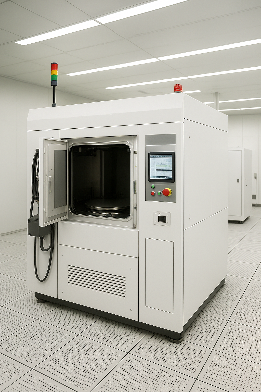
The semiconductor sector constantly stretches the limits of engineering and materials science. From deposition tools to plasma etchers, every piece of equipment relies on parts that can endure extreme temperatures, reactive chemistries, and continuous mechanical stress. At the same time, equipment manufacturers face pressure to shorten development cycles and deliver prototypes quickly to support new device architectures and packaging technologies.
Top Seiko addresses both of these challenges through two key capabilities: expertise in machining advanced materials and the ability to deliver precision prototypes on accelerated timelines.
Engineering with materials that others can’t handle
Many of the components used inside semiconductor manufacturing tools cannot be made from conventional metals or polymers. Top Seiko specializes in processing high-performance materials that are often the only viable choice for these demanding environments, such as:
Technical ceramics, fused quartz, carbides, and refractory metals that maintain purity and performance under harsh conditions
Chamber liners, shields, and internal parts that resist plasma erosion and extend tool lifetimes
Susceptors, carriers, and wafer handling stages that remain stable under high heat
Gas delivery nozzles and injectors designed for precise flow control even in corrosive atmospheres
Custom fixtures and jigs supporting test, measurement, and assembly processes
By ensuring longer component life and more consistent operating conditions, Top Seiko helps OEMs lower maintenance costs and improve yield reliability.
Prototyping without delays
In semiconductor R&D, speed is just as vital as durability. When engineers are validating a new chamber layout or running first trials of a process recipe, waiting months for a single part can stall progress.
Top Seiko helps its customers move faster by providing:
Short lead times, thanks to flexible machining setups
Accurate one-offs and low-volume runs, ideal for prototypes and pilot production
Close engineering collaboration, so design tweaks and manufacturability feedback happen quickly
This means customers can test earlier, refine designs faster, and ultimately launch new process capabilities ahead of the competition.
Why semiconductor OEMs count on partners like Top Seiko
The global equipment supply chain is built on collaboration. Large system manufacturers concentrate on integration and system performance, while specialists like Top Seiko provide the high-value parts that keep these tools running at their best.
By uniting deep knowledge of hard-to-machine materials with agile prototyping services, Top Seiko reinforces the semiconductor innovation ecosystem. Customers don’t just get precision parts—they gain a partner who understands the urgency of staying ahead in a fast-moving industry.
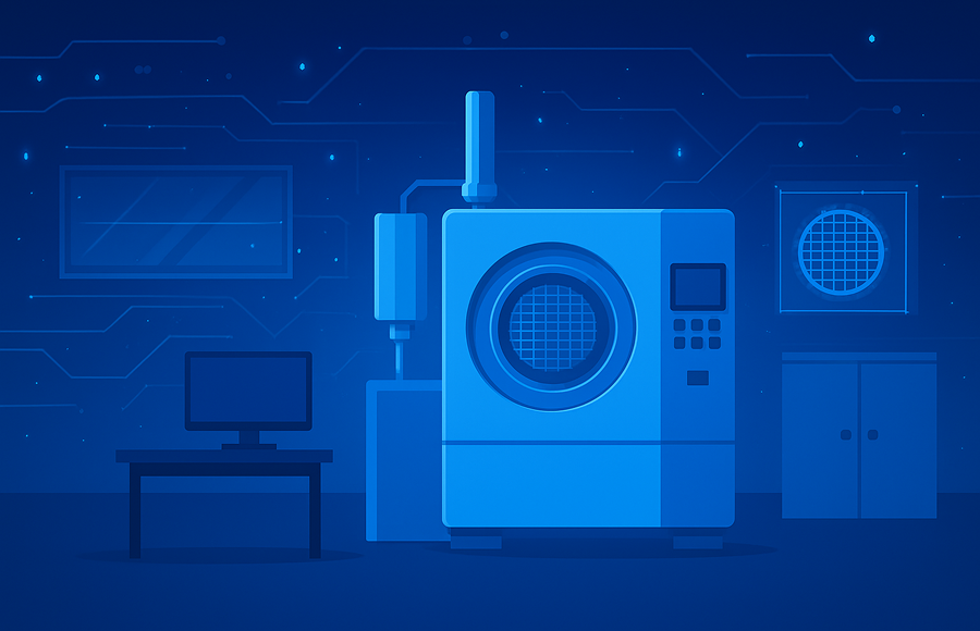
AI-created realistic image showing next-generation semiconductor manufacturing equipment in a cleanroom, with focus on lithography and etching modules.
In essence: Top Seiko is more than a parts supplier. It is a trusted partner enabling faster development and greater reliability for leading semiconductor equipment makers worldwide.
Looking for a solution that integrates precision and performance?
We’d be happy to talk.
![]()
![]()


